Xilinx Kintex-7 FPGA Embedded Kit
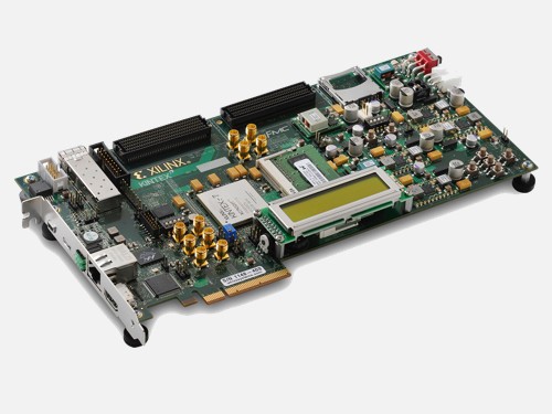
The Kintex®-7 Embedded Kit includes the components of the Kintex-7 KC705 Base Evaluation Kit plus all additional soft content that embedded designers need to quickly design their high-performance embedded systems.
Overview
Product Description
The Kintex®-7 Embedded Kit includes the components of the Kintex-7 KC705 Base Evaluation Kit plus all additional soft content that embedded designers need to quickly design their high-performance embedded systems. This includes the embedded targeted reference design and relevant tools such as Vivado® Design Suite.
Key Features & Benefits
- Supports embedded processing with MicroBlaze, soft 32bit RISC
- Leverages the Kintex-7 KC705 base board
- Familiar Eclipse-based integrated development environment (IDE), GNU tools, operating systems, libraries and a pre-verified reference design
Featured Xilinx Devices
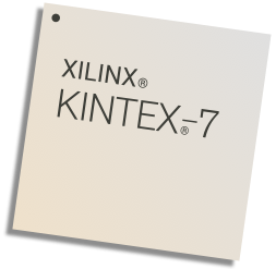
Featuring the ROHS compliant KC705 kit including the XC7K325T-2FFG900C FPGA
| Logic Cells | 326,080 |
|---|---|
| DSP Slices | 840 |
| Memory | 16,020 |
| GTYX Transceivers | 16 |
| I/0 Pins | 500 |
Product Information
Board Features
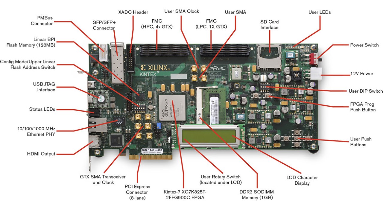
Featuring the Kintex-7 Embedded Board
Configuration
- Onboard JTAG configuration circuitry to enable configuration over USB
- JTAG header provided for use with Xilinx download cables such as the Platform Cable USB II
- 128MB (1024Mb) Linear BPI Flash for PCIe Configuration
- 16MB (128Mb) Quad SPI Flash
Memory
- 1GB DDR3 SODIMM 800MHz / 1600Mbps
- 128MB (1024Mb) Linear BPI Flash for PCIe® Configuration
- 16MB (128Mb) Quad SPI Flash
- 8Kb IIC EEPROM
- SD card slot
Communication & Networking
- Gigabit Ethernet GMII, RGMII and SGMII
- SFP / SFP+ cage
- GTX port (TX, RX) with four SMA connectors
- UART to USB bridge
- PCI Express x8 edge connector
Display
- HDMI video output
- External Phy/codec device driving an HDMI connector
- 2x16 LCD display
- 8x LEDs
Clocking
Used to support CPRI/OBSAI applications that perform clock recovery from a user-supplied SFP/SFP+ module
- Fixed Oscillator with differential 200MHz output used as the “system” clock for the FPGA
- Programmable Oscillator with 156.250 MHz as the default output and frequency targeted for Ethernet applications but oscillator is programmable for many end uses
- Differential SMA clock input
- Differential SMA GTX reference clock input
- Jitter attenuated clock used to support CPRI/OBSAI applications that perform clock recovery from a user-supplied SFP/SFP+ module
Expansion Connectors
- FMC-HPC (partial population) connector (4 GTX transceiver, 116 single-ended or 58 differential (34 LA & 24 HA) user defined signals)
- FMC-LPC connector (1 GTX transceiver, 68 single-ended or 34 differential user defined signals)
- Vadj can support 1.8V, 2.5V, or 3.3V
- IIC
Power
- 12V wall adapter or ATX
- Voltage and current measurement capability of 2.5V, 1.5V, and 1.2V, 1.0V supplies (IIC path to FPGA)
Analog
- XADC header
Control & I/O
- 5X push buttons
- 4X DIP switches
- Diff pair I/O (1 SMA pair)
- AMS FAN header (2 I/O)
- 7 I/O pins available through LCD header
What's Inside
KC705 Evaluation Board
Featuring the XC7K325T-2FFG900C FPGA
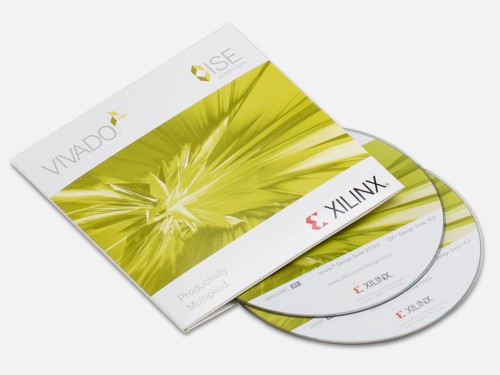
Full seat Vivado® Design Suite: Design Edition
Node locked & Device-locked to the Kintex-7 XC7K325T FPGA, with 1 year of updates
AMS 101 Evaluation Card
Pairs with free AMS Evaluator tool for analyzing analog data, internal temperature and voltage measurements, and saving data to a .csv file
Ethernet Cable
USB Micro Cable
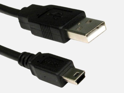
USB Mini Cable
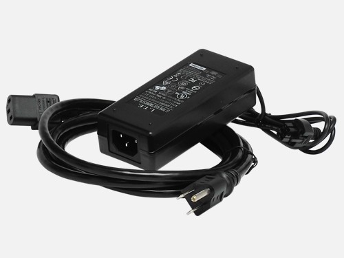
Power Cord and Power Adapter
Resources
Design Tools
| Name | Description | License Type |
|---|---|---|
| Vivado Design Suite Design Edition | The Xilinx Vivado® Design Suite is a revolutionary IP and System Centric design environment built from the ground up to accelerate the design for FPGAs and SoCs. | Node locked & Device-locked to the Kintex-7 XC7K325T FPGA, with 1 year of updates |
Intellectual Property
| Name | Description | License Type |
|---|---|---|
| Memory Interface Generator (MIG) | MIG is a free software tool used to generate memory controllers and interfaces for Xilinx FPGAs. | No-Charge IP |
| logiCVC-ML Compact Multilayer Video Controller | The logiCVC-ML – Compact Multilayer Video Controller is a graphics controller optimized for Xilinx FPGAs and Zynq®-7000 SoCs. It controls LCD TFT flat panel displays and, by means of external video converters, S-Video, Composite Video devices and CRT displays. | 1 hour hardware timeout |
| logiSDHC SD Card Host Controller | The logiSDHC is the Secure Digital (SD) card Host Controller IP core from the Xylon logicBRICKS IP core library. It is designed to transfer data from the system memory to the SD card's data bus, and vice versa. | 1 hour hardware timeout |
Additional Tools, IP and Resources
| Name | Product Category | Item | Description |
|---|---|---|---|
| Partners | Operating System | Partner Operating System & Tool Solutions for MicroBlaze | A list of 3rd party embedded solutions providers including OS and more |
| Open Source | Software Tool | TeraTerm | One of many possible terminal emulators used for serial connection from your PC to the evaluation kit. |
| Xilinx | Software Tool | TeraTerm | SDK environment that works with Xilinx Hardware to build, develop, test and deploy a embedded Linux solution. |

