AR# 34589
|MIG Virtex-6 DDR2/DDR3 - General Board Level Debug
描述
This Answer Record provides information on general board level debug for DDR2/DDR3 design using MIG.The information provided in this Answer Record should be the starting point in any hardware debug of a memory interface design.
NOTE: This Answer Record is part of the Xilinx MIG Solution Center (Xilinx Answer 34243). The Xilinx MIG Solution Center is available to address all questions related to MIG. Whether you are starting a new design with MIG or troubleshooting a problem, use the MIG Solution Center to guide you to the right information.
解决方案
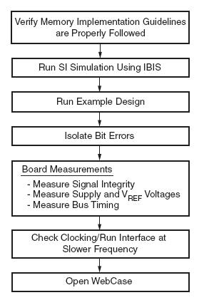
Following is the recommended flow for debugging a hardware issue involving a memory interface:For detailed information on Verify Memory Implementation Guidelines, refer to:
Each of these steps is detailed in the Debug Guide provided with The Virtex-6 FPGA Memory Interface Solutions User Guide. Go to the DDR2 and DDR3 SDRAM Memory Interface Solution > Debugging Virtex-6 FPGA DDR2/DDR3 SDRAM Designs > Hardware Debug section.
To open a WebCase, go to:
http://www.xilinx.com/support/clearexpress/websupport.htm
链接问答记录
相关答复记录
| Answer Number | 问答标题 | 问题版本 | 已解决问题的版本 |
|---|---|---|---|
| 34544 | MIG Virtex-6 DDR2/DDR3 - Board Layout | N/A | N/A |
| 34588 | MIG Virtex-6 DDR2/DDR3 - Board Debug including general debug, calibration debug, and data error debug | N/A | N/A |
| 34308 | MIG Virtex-6 DDR3/DDR2 - Verify pin-out/banking requirements are met | N/A | N/A |
