AR# 47817
|Design Advisory for the Kintex-7 and Virtex-7 GTX Transceiver Power-up/Power-down
描述
This answer record discusses the 7 series FPGAs GTX Transceiver power-up/power-down sequencing recommendations and its implications.
解决方案
1) Recommended power-up/power-down sequence:
The recommended GTX transceiver power-on sequence is VCCINT, VMGTAVCC, VMGTAVTT or VMGTAVCC, VCCINT, VMGTAVTT to achieve minimum current draw. There is no recommended sequencing for VMGTVCCAUX. Both VMGTAVCC and VCCINT can be ramped up simultaneously. The recommended power-off sequence is the reverse of the power-on sequence to achieve minimum current draw.
If the recommended sequences are not met, current drawn from VMGTAVTT can be higher than specifications during power-up and power-down:
- When VMGTAVTT is powered up before VMGTAVCC, and VMGTAVTT - VMGTAVCC > 150 mV and VMGTAVCC < 0.7V, the VMGTAVTT current draw can increase by 460 mA per transceiver when VMGTAVCC is ramping up. The duration of the current draw can be up to 0.3* TMGTAVCC (ramp time from GND to 90% of VMGTAVCC).
- When VMGTAVTT is powered up before VCCINT , and VMGTAVTT - VCCINT > 150 mV and VCCINT < 0.7V, the VMGTAVTT current draw can increase by 50 mA per transceiver when VCCINT is ramping up. The duration of the current draw can be up to 0.3* TVCCINT (ramp time from GND to 90% of VCCINT).
- When VMGTAVCC is powered down before VMGTAVTT, and VMGTAVTT - VMGTAVCC > 150 mV and VMGTAVCC < 0.7V, the VMGTAVTT current draw can increase by 460 mA per transceiver when VMGTAVCC is ramping down. The duration of the current draw can be up to 0.3* TMGTAVCC (ramp time from 100% to 10% of VMGTAVCC).
- When VCCINT is powered down before VMGTAVTT , and VMGTAVTT - VCCINT > 150 mV and VCCINT < 0.7V, the VMGTAVTT current draw can increase by 50 mA per transceiver when VCCINT is ramping down. The duration of the current draw can be up to 0.3* TVCCINT (ramp time from 100% to 10% of VCCINT).
2) For the 7 Series GTX Transceiver General ES Silicon ONLY:
Please note that this section does not apply to GTX Production silicon.
2 a) If the recommended power sequences are not met, then the GTX transceiver can become inoperative if both of the following conditions occur at the same time:
- VMGTAVTT is within its recommended operating range
AND - VMGTAVCC is at a voltage less than 0.4V for more than 10,000 cumulative hours
An additional 100 mA per transceiver is drawn from VMGTAVTT when VMGTAVTT is within its recommended operating range and VMGTAVCC is at a voltage of 0.4V or less.
2 b) If the recommended power-up sequence is followed, while VMGTAVCC is powered within its recommended operating range and VMGTAVTT is below 0.7V, an additional 50 mA per GTX transceiver is drawn from VMGTAVCC. Depending on the number of transceivers used, this extra current could be greater than reported in XPE.
Follow this procedure to determine if the power supply regulator for VMGTAVCC is sufficient:
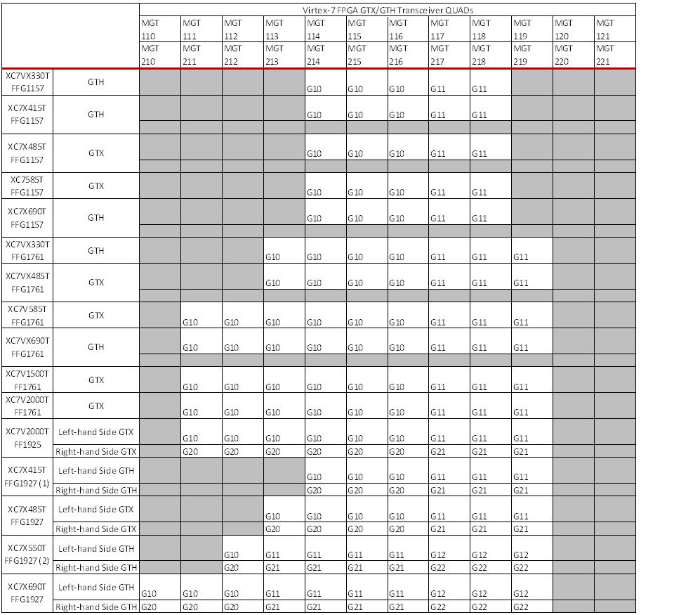
- Refer to Table 5-2 Kintex-7 FPGA GTX Transceiver Power Supply Grouping Per Package in the 7 Series FPGAs GTX/GTH Transceivers User Guide (UG476) and Table 1 Virtex-7 FPGA GTX/GTH Transceiver Power Supply Grouping Per Package to determine the total number of QUADs per power supply grouping
- Refer to Table 2: Total GTX VMGTAVCC Current for Number of QUADs in a Power Supply Grouping to determine the maximum VMGTAVCC current per power supply grouping.
- Calculate the VMGTAVCC power consumption per power supply grouping based on the number of transceivers used using XPE.
- If the current value obtained from XPE in Step 3 is greater than or equal to the current value obtained in Step 2, no change is required.
- If the current value obtained from XPE in Step 3 is less than the current value obtained in Step 2, it is recommended that the power supply regulator for VMGTAVCC be enhanced to account for this extra current.
Table 1: Virtex-7 FPGA GTX/GTH Transceiver Power Supply Grouping Per Package

Notes:
- Power Pins and Pinout for QUAD113 and QUAD213 are made available for seamless migration/swapping to the XC7VX485T, XC7VX550T and the XC7VX690T.
- Power Pins and Pinout for QUAD110, QUAD210, QUAD111 and QUAD211 are made available for seamless migration/swapping to the XC7VX550T.
Table 2: Total GTX VMGTAVCC Current for Number of QUADs in a Power Supply Grouping
Number of QUADs in a Power Supply Group
|
VMGTAVCC Current per Power Supply Group (mA)
|
| 6 | 1200
|
| 4 | 800
|
| 3 | 600
|
| 2 | 400
|
| 1 | 200
|
3) Frequently Asked Questions
1) What should these additional currents be added to when not following the recommended sequences?
For GTX Production Silicon, this assumes that XPE 14.2 version or newer is used. For GTX General ES silicon, this assumes that XPE 13.4 version or newer is used.
- If the recommended sequence is used, there are no additional currents to be added.
- If the recommended sequence is not used, then the additional currents mentioned are added on top of the XPE numbers.
2) Simultaneous power-up: Is it okay to simultaneously power-up VMGTAVCC and VMGTAVTT, OR VCCINT and VMGTAVTT, OR all three? Does the additional current draw still apply?
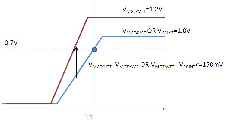
- During power-up, if VMGTAVCC < 0.7V (Time "T1" in the picture) and VMGTAVTT - VMGTAVCC <= 150 mV, then there is no additional current draw. During power-up, if VMGTAVCC >= 0.7V (Time "T1" in the picture), then there is no additional current irrespective of VMGTAVTT value.
- During power-up, if VMGTAVCC < 0.7V (Time "T1" in the picture) and VMGTAVTT VCCINT <= 150 mV, then there is no additional current draw. During power-up, if VCCINT >= 0.7V (Time "T1" in the picture), then there is no additional current irrespective of VMGTAVTT value.
If these conditions cannot be met, then the additional current needs to be accounted for.

3) Are these additional currents on VMGTAVTT cumulative when both sequences of VMGTAVTT vs VMGTAVCC and VMGTAVTT vs VCCINT are not followed?
The power supply current increase is cumulative. So, if both conditions occur simultaneously, the total is 510mA (460 mA + 50 mA) extra on VMGTAVTT for Production silicon and 610 mA (460 mA + 50 mA + 100 mA) extra on VMGTAVTT for General ES silicon when conditions in section 2.1 also apply.
4) What is the impact of this additional current and when does this happen?
This additional current happens only on the power-up and power-down ramp. Once the GTX transceivers are powered up and running, then this has no impact.
5) What are the key things to keep in mind for the recommended power sequencing to avoid the additional current draw?
VMGTAVTT must be powered up last. VMGTAVCC and VCCINT must be powered up before VMGTAVTT but they can be in any order. VMGTAVCCAUX has no recommended sequencing. These are the criterion that ensure the recommended sequencing is met and there is no current draw.
Revision History
| 10/20/2016 | Added conditions for additional current draw during power-down |
| 07/23/2012 | More clarification added; updated with information on additional current draw when following recommended sequence, duration of current draw, simultaneous power-up and more FAQs. |
| 06/28/2012 | Initial release |
链接问答记录
相关答复记录
| Answer Number | 问答标题 | 问题版本 | 已解决问题的版本 |
|---|---|---|---|
| 42946 | Kintex-7 FPGA 设计咨询主答复记录 | N/A | N/A |
| 41613 | 7 Series FPGAs GTX/GTH Transceivers - Known Issues and Answer Record List | N/A | N/A |
| AR# 47817 | |
|---|---|
| 日期 | 10/26/2016 |
| 状态 | Active |
| Type | 设计咨询 |
| 器件 | |