AR# 50537
|SelectIO Design Assistant - Debugging interfaces between chips that do not give expected digital values. Best Practices for Signal Integrity Debugging
描述
When interfaces between two Integrated Circuits fail, debugging can be difficult.
This Answer Record attempts to give some basic guidance on practices to help capture useful debug information to help identify board level issues.
The following topics are covered within this Answer Record:
- How to verify/identify Signal Quality issues through Simulation and Scope shots
- Tips for isolating Signal Quality as the source of the issue
- Things to look out for.
For a detailed guidance on power and signal integrity analysis and debug, please see the Hardware Debug Guide in (Xilinx Answer 62181).
解决方案
When facing a board level issue that appears to be related to the interface quality between two Integrated Circuits, one common starting point is to physically monitor the quality of the signal with an Oscilloscope.
Because Oscilloscopes are developed for a wide variety of applications, not all Oscilloscope and probes are appropriate for high speed signal quality debugging.
Look for the following in your measurement setup:
- As a general rule of thumb, bandwidth of scope should be at least 5x your fastest frequency content present in your interface.
In modern FPGAs, a 1ns edge rate is a relatively slow edge rage, so a 2.5Gs/sec scope or faster should be used (using rising edge + falling edge as your period and multiplying by 5 as your rule of thumb factor).
Note: This is a rule of thumb. Scope vendors will often just specify a bandwidth where their scope is effective.
- Avoid probes that have long GND leads and a high capacitance. For high speed interfaces, active probes (<1pf) with small GND leads have the lowest impact on the signal you are trying to capture.
If you do notice signal quality improving when a probe is attached to the signal, it might be that the probe's capacitance is filtering problems from the signal.
This is an indicator that 1) your probe is affecting the capture so the scope data is not accurate 2) the signal edges are non-monotonic and you should check your board design.
- Probe as close to the receiver as possible.
Generally, the best spot is the via that connects the receiver, which is generally found inside the BGA grid on the underside PCB below the receiving device.
For a variety of reasons, this is not always possible, but try to probe as close to the receiver as the board allows.
With Scope Shots captured, here are a few common things to look for.
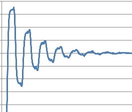
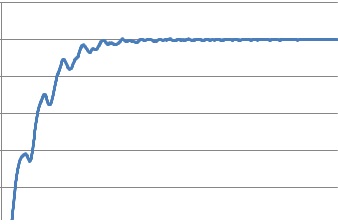
1) Does your signal not cleanly settle at its steady state value? (note: this can happen on rising edges, falling edges, or both (only rising examples are shown below)
Check your termination scheme is appropriate for the standard you are using, and see (Xilinx Answer 47504).


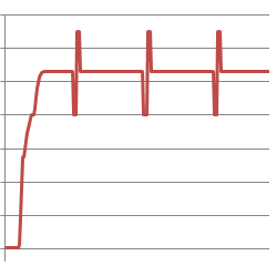
2) Does the Digital data look solid, but do you see a blip on the rising or falling edges?
In this instance you might be looking at a capacitive reflection from the die, see (Xilinx Answer 47504).

3) When the signal is supposed to be a steady logic '1' or steady logic '0', do you see perturbances in the level that somehow relates to I/O switching on the board?
Look at adjacent signals to see if they could be coupling to the trace you are probing, check Simultaneously Switching limits are not violated (Xilinx Answer 31905), and ensure decoupling on the Vcco rail meets User Guide recommendations for the device you are using.

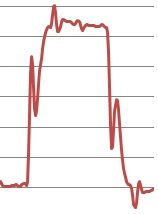
4) For any other unexpected shapes in your scope shots, it is often useful to isolate that feature to a location on your PCB.
Using the rule of thumb of 180ps/inch, most perturbances will occur either delayed in time, or lasting for a time that correlates to a feature on your PCB.
For example if you have a perturbance that lasts 180ps, try looking for features on your PCB that might be an inch long.
5) Are there reflections on the line? Is there ringing on the line?
Is the Signal not crossing the thresholds at the receive side?
Reflections and ringing are usually caused by impedance mismatching on the transmission line.
Perform an IBIS simulation to see if the reflections in simulations are the same as on hardware, try the Fast-Strong and Slow-Weak process corners, and look at the Pin and the Die.
If the reflections are seen at the pin but not at the die, then there is not an issue. See (Xilinx Answer 47504) for more information.
If there are still reflection seen by the die, then there is an impedance mismatch on the line. Try running the Termination Wizard in the IBIS simulator (if available), ensuring that the simulation correctly reflects the hardware.
For example, include vias, PCB information like Stackup, and the other signals around the "victim" signals.
General Debug steps / questions:
Check the Vcco and Gnd rails.
Take an oscilloscope of the rails with persist on when the interface is running.
If there is access to the test pins, perform a spy hole measurement where the design continually drives out a Logic high on test pins and scope these pins (the beginning of the Answer Record provides details on Oscilloscopes).
Ground or power bounce can occur when a large number of outputs simultaneously switch in the same direction.
It is an important step to ensure that the design passes a SSN analysis.
For details on SSN analysis see (Xilinx Answer 31905).
Check the terminations. For details on terminations see (Xilinx Answer 47225).
Perform an IBIS or Spice simulation. For details on IBIS simulations see (Xilinx Answer 50644).
Board is experiencing receive errors:
If a board is experiencing receive errors on hardware, there can be many root causes.
Details of the transmitter if the FPGA is the transmitter:
To build up a clear picture of the system is it useful to understand the details of how the outputs are driven.
Is it an OSERDES, ODDR?
What clocking topology is used, for example, CCIO driving BUFIO/BUFR combination, BUFR diving by X.
Is an output delay used? What attributes are used?
Details of the input clock? for example, scope shots of the input clock including jitter characteristics.
Timing Report details (please include timing report).
Details of the receiver:
Measurements are usually taken at the receiver, therefore it is also useful to understand what is happening at the receive side.
What receiver is used? ISERDES, IDDR, etc. If an ISERDES is used, what are the attributes which are used. (mainly INTERFACE_TYPE)
Is an input delay used? What attributes are used?
Also, details of the input clock used to receive the data? for example, scope shots of the input clock including jitter characteristics.
This might be the forwarded clock from the transmitter.
How are the receive errors identified? BIST? Calibration failure? Please provide details on how the receive errors are identified.
If the FPGA is the receiver please also include ChipScope shot showing the errors.
Timing Report details, please include timing report.
Try reproducing the issue in a testcase, strip the design down to the failing interface. Does it still fail? If possible include the testcase in the Technical Support Service Request.
After gathering this information please create a Service Request including the details in the Technical Support SelectIO Service Request checklist listed at the end of the answer record.
Open a Service Request from the support page:
https://www.xilinx.com/support.html#serviceportal
Technical Support Service Request checklist:
- What device, speed grade, and package is being used?
- What IOSTANDARD is being used at what frequency?
- Termination details, DCI or on board. What the Vrp & Vrn are connected to and what is the value of the reference resistors. Also if DCI cascade is used?
- Scope shots of the signal experiencing the issue
- Scope shots of Vcco, GND. If the IOSTANDARD uses Vref and the internal Vref is used also include a scope shot of Vccaux.
- IBIS simulation outputs. Also if possible, the schematic to reproduce the IBIS simulation.
- Pad report
- Details of the device interfacing to the Xilinx FPGA
Other miscellaneous details that can also be beneficial:
- How many boards experience the issue? Out of how many?
- Are there any temperature variations?
- If you increase the Vcco (within the data sheet specified limits) does this improve the behavior?
- Details on the decoupling of the FPGA on the board
链接问答记录
主要问答记录
| Answer Number | 问答标题 | 问题版本 | 已解决问题的版本 |
|---|---|---|---|
| 50926 | Xilinx SelectIO Solution Center - Design Assistant | N/A | N/A |
子答复记录
| Answer Number | 问答标题 | 问题版本 | 已解决问题的版本 |
|---|---|---|---|
| 31905 | Simultaneously Switching Noise - Where can I find documentation on SSO/SSN? | N/A | N/A |
| 47225 | SelectIO Design Assistant - How to Terminate a Transmission Line | N/A | N/A |
| 47504 | SelectIO Design Assistant - Debug hardware issue with on-chip termination | N/A | N/A |
| 50644 | SelectIO Design Assistant: IBIS Models & Simulation | N/A | N/A |
| AR# 50537 | |
|---|---|
| 日期 | 06/13/2017 |
| 状态 | Active |
| Type | 综合文章 |
| 器件 | |