AR# 46880
|Zynq-7000 Example Design - Linear QSPI Performance (Max Effective Throughput)
描述
This example design shows how to achieve QSPI (in Linear Mode) Maximum Effective Throughput with a 100 MHz SPI clock.
Note: An Example Design is an answer record that provides technical tips to test a specific functionality on Zynq-7000.
A tip can be a snippet of code, a snapshot, a diagram or a full design implemented with a specific version of the Xilinx tools.
It is up to the user to "update" these tips to future Xilinx tools releases and to "modify" the Example Design to fulfill his needs.
Limited support is provided by Xilinx on these Example Designs.
| Implementation Details | |||
|---|---|---|---|
| Design Type | PS only | ||
| SW Type | Standalone | ||
| CPUs | Single CPU @ 720MHz | ||
| PS Features | QSPI ( in linear mode) with SPI clock @ 100MHz | ||
| PL Cores | -- | ||
| Boards/Tools | ZC702 (modified to have MIO[8] n.c. in order to enable the qspi loopback). | ||
| Xilinx Tools Version | EDK 14.1 | ||
| Other details | -- | ||
| Files Provided | |||
| xdmaps_example_w_intr_14_2.c | Snippet of code. | ||
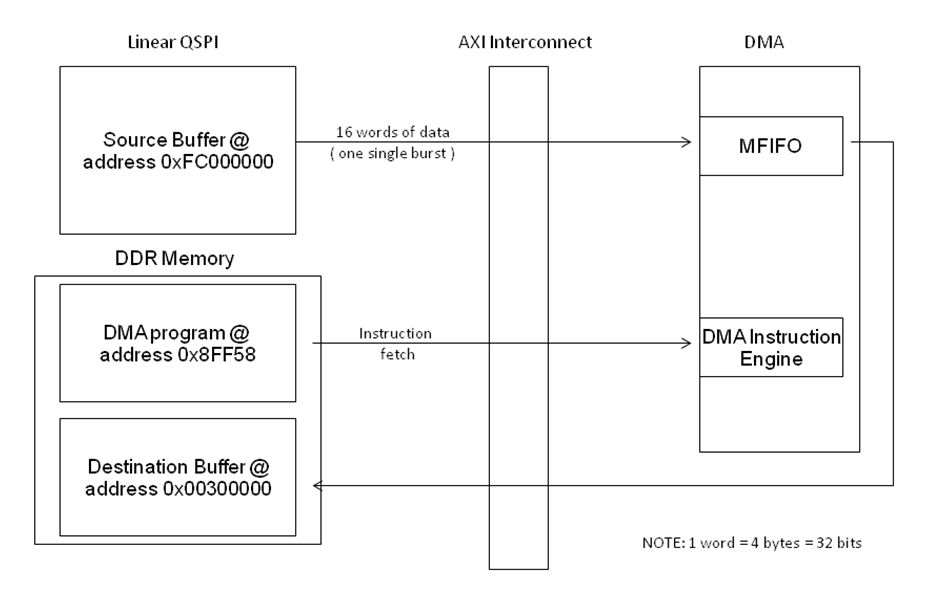
| Block Diagram | |||
 | |||
解决方案
Overview
In order to achieve Linear Mode Maximum Effective Throughput with 100 MHz SPI clock, the DMA controller has been used.
This very flexible DMA can execute a few lines of microcode in order to transfer data from the Linear QSPI to DDR.
Below is an example of microcode that moves 256 Kbytes from LQSPI to DDR:
DMAMOV CCR, SB16 SS32 DB16 DS32
DMAMOV SAR, 0xFC000000
DMAMOV DAR, 0x00300000
DMALP 256
DMALP 256
DMALD
DMAST
DMALPEND
DMALPEND
DMAEND
The QSPI is set to operate in Linear Mode: single SPI flash memory, Fast read quad I/O (LQSPI_CFG = 0x82FF04EB ).
SPI reference clock: 200 MHz
SPI clock: 100 MHz (with DIV2)
The CPU is running at 720 MHz and DDR at 533 MHz.
Transfer time is calculated by counting elapsed counter ticks in the CP15 performance monitor register.
Step-by-step Instructions
- Open Xilinx SDK.
- Create a Zynq Empty Application Project.
- Import the attached xdmaps_example_no_intr.c (modified from the example provided by the tools to accommodate LQSPI):
- Be sure that SRC_LQSPI is defined and PROCESSOR_TICKS_TO_US matches your system settings.
Note: I also attached an example tested on 14.2.
It does not include the "transfer time" calculation, but it shows how to use the DMA to read data from the qspi.
Expected results
Following are the results for 1.0 silicon:
| Read mode at 100 MHZ (DIV2) | Average PL330 transfer time to DDR (MBytes/sec) | % Bandwidth Vs. theoretical 50 MBytes/sec |
| QUAD OUTPUT - FAST READ (0x6B) | ~ 31 | ~ 62% |
| QUAD IO - FAST READ (0xEB) | ~ 36 | ~ 72% |
附件
| 文件名 | 文件大小 | File Type |
|---|---|---|
| xdmaps_example_w_intr_14_2.c | 12 KB | C |
| xdmaps_example_no_intr.zip | 7 KB | ZIP |
链接问答记录
主要问答记录
| Answer Number | 问答标题 | 问题版本 | 已解决问题的版本 |
|---|---|---|---|
| 51779 | Zynq-7000 SoC - Example Designs and Tech Tips | N/A | N/A |
相关答复记录
| Answer Number | 问答标题 | 问题版本 | 已解决问题的版本 |
|---|---|---|---|
| 50991 | Zynq-7000 SoC - What devices are supported for configuration? | N/A | N/A |
| AR# 46880 | |
|---|---|
| 日期 | 05/18/2018 |
| 状态 | Active |
| Type | 综合文章 |
| 器件 | |
| Tools | |
| Boards & Kits | |