AR# 50194
|SelectIO Design Assistant: Performance - Single Ended I/O Standards
描述
This Article forms part of the Performance section of the Design Assistant (Xilinx Answer 50926) in the SelectIO Solutions Centre (Xilinx Answer 47284).
Please see the main Performance article for more information on I/O performance. (Xilinx Answer 47284)
This article will Discuss the following:
How are single ended I/O standards defined by Xilinx?
What are the main performance specifications for Single ended I/O standards?
解决方案
Single-Ended I/O Standards:
Single-ended signaling is the simplest and most commonly used method for transmitting electrical signals between devices. The signal is represented by a varying voltage on one trace or wire. This is usually referenced to another signal in order to determine the value of the input.
In the case of older standards such as LVCMOS and LVTTL, the reference voltage is usually ground.
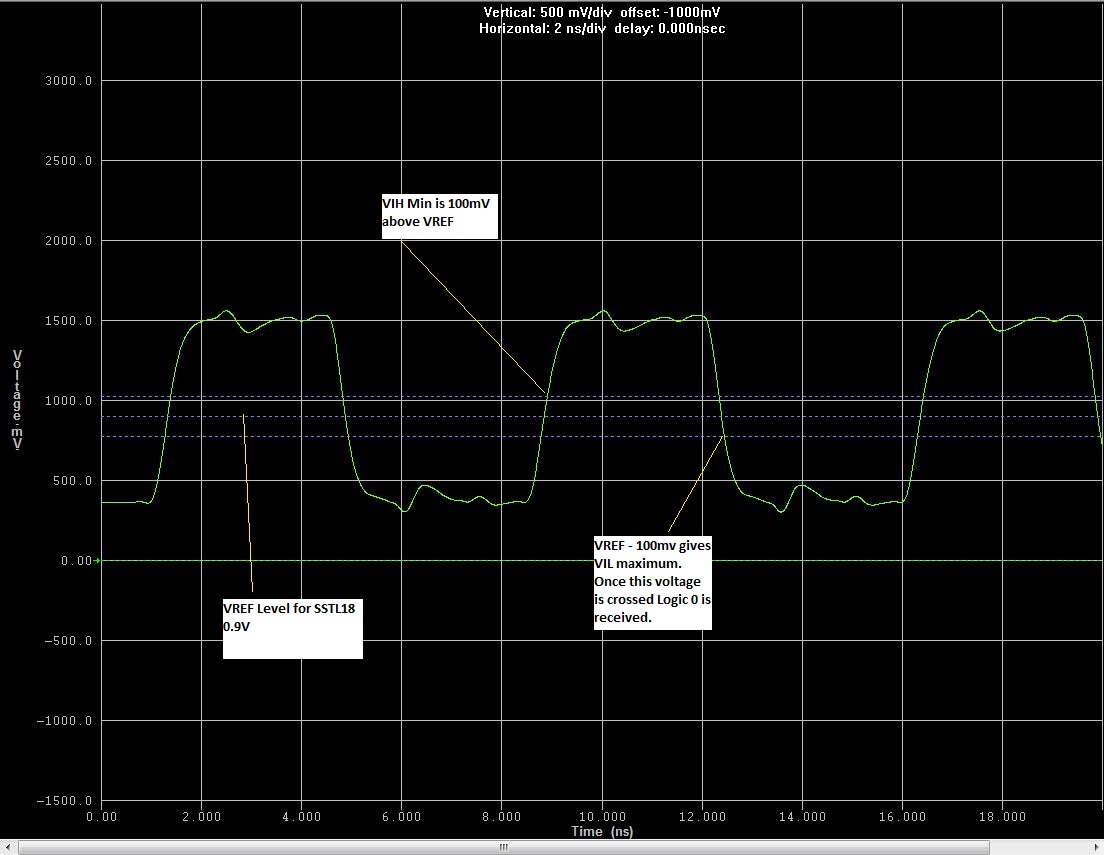
Single ended memory standards such as SSTL and HSTL are referenced to a VREF between 0V and the power supply rail, allowing them to switch faster.
Single-Ended I/O is less expensive to implement and there are fewer PCB traces/Wires per signal, however they suffer from noise on the ground or VREF between the devices and they are likely to be affected by induction with other signals on the board.
The main performance characteristics of Xilinx Single-Ended I/O can be found in the device data sheet.
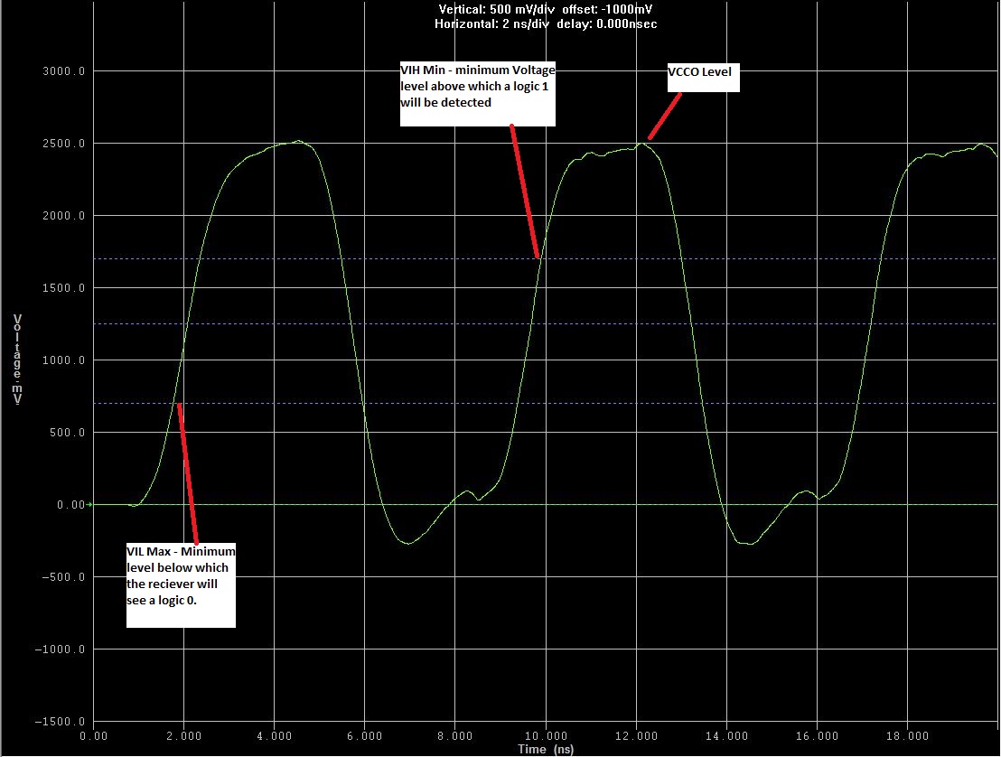
For inputs, there are two main things that we are interested in, namely, at what voltage level does the input switch from low to high and vice versa. These specifications are known as VIL and VIH.
In Xilinx devices the minimum and maximum value for each I/O standard are specified. Once the signal is within the VIL band, the device recognizes a logic 0 at the input and once the signal is in the range of VIH min and VIH max, the receiver will recognize a logic one at the input.
You can see an example of these input levels in the following image.

HSTL/SSTL standards are single ended but they are based around a reference voltage. These types of Standards usually specify their VIL/VIH levels in terms of the VREF.

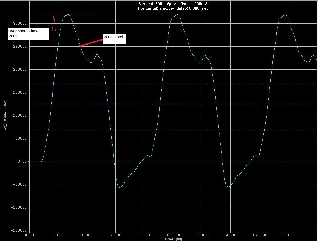
If the driver driving the line is strong (it has a high current drive capability) it can happen that there is overshoot at the receiver.
The absolute maximum ratings in the datasheet for the device usually specify both the level and the duration this overshoot can have.

For outputs, Xilinx also specifies the VOH and VOL figures for its single ended I/Os.
Values for the output current drive, IOL and IOH are guaranteed over the recommended operating conditions at the VOL and VOH test points.
This indicates the load that the I/O can drive and still provide the stated output logic levels.
Drive strength expressed in milliamps is explained in (Xilinx Answer 38820)
These specifications allow you to check that the signal you are driving to the downstream device or the signal you are receiving will be received correctly.
In general, singled ended outputs swing full rail-to-rail at lower speeds, and will reduce in amplitude as frequencies increase. If you need a guaranteed min/max voltage for your particular board/interface, you will need to run your own IBIS or HSPICE simulations, with their particular topography and frequencies. Doing this across PVT corners is the only true way to identify if they will have issues meeting Vil/Vih at their receivers.
链接问答记录
主要问答记录
| Answer Number | 问答标题 | 问题版本 | 已解决问题的版本 |
|---|---|---|---|
| 47284 | SelectIO Design Assistant: Performance | N/A | N/A |
相关答复记录
| Answer Number | 问答标题 | 问题版本 | 已解决问题的版本 |
|---|---|---|---|
| 13781 | Virtex-II, XCITE/DCI - What is the slew rate or drive strength of LVDCI I/O? | N/A | N/A |
| 39681 | Spartan-6 FPGA - What is the input signal transition time or Tin? | N/A | N/A |
| AR# 50194 | |
|---|---|
| 日期 | 06/02/2017 |
| 状态 | Active |
| Type | 解决方案中心 |
| 器件 | |