AR# 50653
|SelectIO Design Assistant: IBIS Models & Simulation - IBIS Model Background
描述
This article deals with IBIS models for I/Os. It is intended to explain the IBIS model structure and how the simulation model represents the behavior of the I/O.This article is part of the Design Assistant section (Xilinx Answer 50926) of the SelectIO Solution Centre (Xilinx Answer 50924).
解决方案
Due to the increased likelyhood of encountering Signal Integrity problems at higher I/O frequencies, the need to simulate these interfaces before prototyping becomes essential.
In order to simulate a board interface, all of the components on the board associated with that interface need to be modeled. The IBIS (I/O Buffer Interface Specification) is an electrical model standard used to define component models for board components (integrated circuit buffers, connectors, and transmission lines) in a behavioral syntax that has become widely accepted among EDA vendors.
IBIS stands for Input/Output Buffer Information Specification. It is defined by the Electronics Industry Alliance. It provides a table-based model for I/O switching and passive component behavior.
IBIS models of integrated circuits (ICs) consist of I/V output curves, rising/falling transition data, and package parasitic information of the device.
IBIS models are intended to provide information about I/O buffer electrical characteristics, but are not typically used to calculate delay information for system or board-level timing analysis.
Xilinx SelectIO IBIS models are extracted from the HSPICE models of the actual I/O circuitry of the device family.
IBIS introduced the baseline architecture associated with most CMOS, BiCMOS and TTL technologies.
The following features were included:
- Human-readable ASCII file format (.ibs) with header information
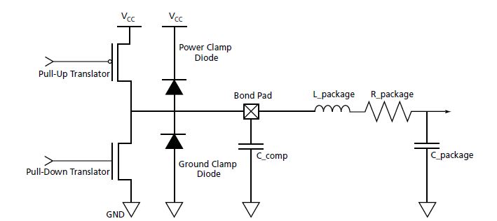
- Components (pinout) and default Package model L_pkg, R_pkg, C_pkg
- Pin specific model selection and L_pin, R_pin, C_pin
- Models (electrical)
- Model_types (Input, Output, 3-state, I/O, Open_drain)
- Pull-up, Pull-down, Gnd Clamp, Power Clamp I/V tables relative to voltages
- Ramp dV/dt_r, dV/dt_f for defining rising and falling transitions
- C_comp for die capacitance
- Typ-Min-Max columns for performance corners
- Defined conditions for temperature and transition load
CMOS I/O models in IBIS are typically represented as shown below:

Note that the input buffer is not present - this is because most CMOS input buffer circuits are very high-impedance, and the only relevent information for signal integrity modeling purposes is the input switching thresholds (which are provided for any input or bidirectional pin).
Model File Structure
Each Xilinx IBIS model file will have a header section. This contains information about the following:
- The IBIS Version
- The Model Revision
- The source, i.e. the Spice model that the IBIS model was extracted from
- Disclaimer
- Copyright
There is then some device information, namely the component name and some basic package parasitic parameters.
The R_pkg, L_pkg, and C_pkg values represents default package parasitic values associated with the device package pins.
After the component package information, the IBIS model contains the [Pin] mapping section. Each pin in this section is mapped to a device buffer model. For Xilinx FPGAs, there are many different I/O standards that are supported, and supporting all of these I/O standards was accomplished by assigning each supported I/O standard and feature to the different pins in the family-specific IBIS model file.
The mapping section selects the correct model for the IOSTANDARD, for example DIFF_SSTL12_T_DCI_S_HP_O_P maps to the SSTL12_DCI_S_HP_O model as this is the equivalent model for the driver, DIFF_SSTL18_I_S_HP_P and DIFF_SSTL18_I_S_HP_N both map to SSTL18_I_S_HP as they are complementary single-ended IOSTANDARD and the equivalent model is SSTL18_I_S_HP.
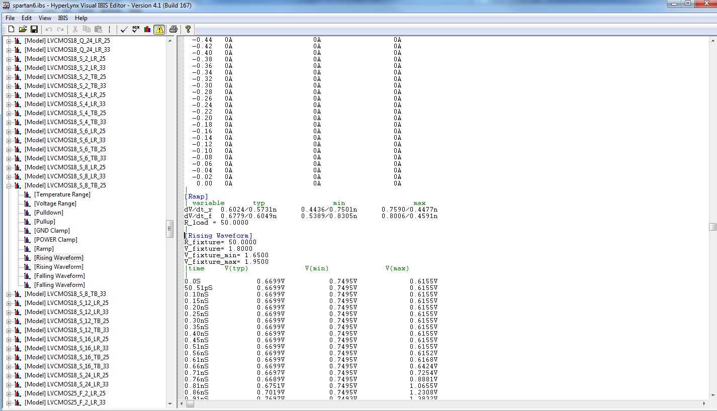
After this section the file contains the [Model] section where the individual I/O standard models are included. The top of each [Model] section contains information about the model type (I/O, input-only, output-only, etc), polarity, enable pin, input thresholds (Vinl/Vinh), reference parasitic information related to extraction circuit, and the total capacitance of the I/O pad (C_comp).
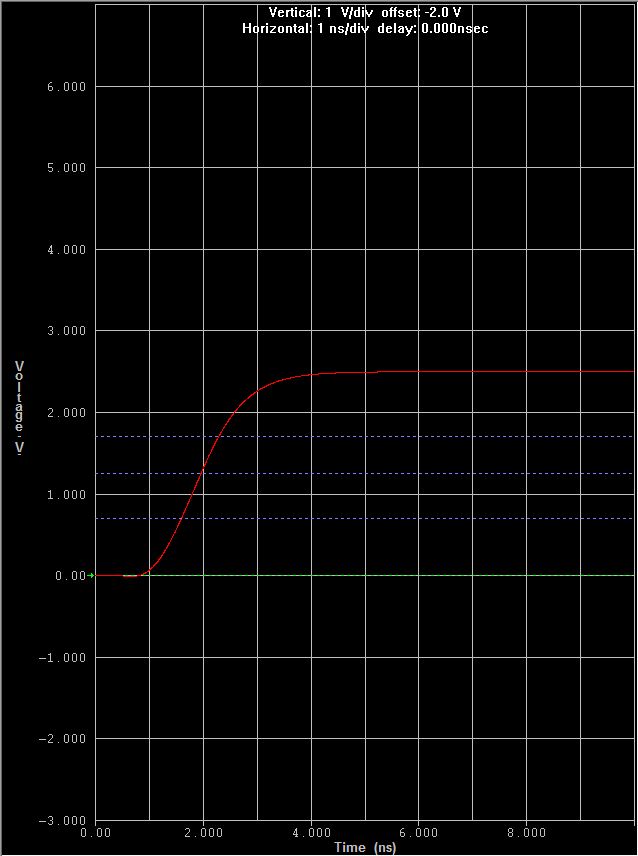
For each model in the [Model] section, the pull-up and pull-down transistors of the output buffer are then represented by DC I/V characteristic tables ([Pullup] and [Pulldown]), and AC V/T tables ([Rising Waveform] and [Falling Waveform]). For each of these tables, the data is provided for three corners: typ, min, and max.
The overall signal behavior of the I/O pin is largely determined from these four tables.
There are also [GND Clamp] and [POWER Clamp] tables, which represent the ESD and clamping diode properties.
These tend to effect the signal behavior whenever the pin has overshoot.
IBIS model file viewer tools contain the ability to plot out the I/V and V/T tables - as show below for an example of the [Rising Waveform]:


Package Parasitics:
For IBIS models extracted from a design in the Xilinx tools, there will be a set of package parasitics included in the model. This will give a more complete picture of the how the signal propagation will work in the design.
IBIS models and HSPICE:
For more information on the difference between IBIS and SPICE models and where they can be downloaded please see (Xilinx Answer 2932)
For more general information on IBIS models please see (Xilinx Answer 3359)链接问答记录
主要问答记录
| Answer Number | 问答标题 | 问题版本 | 已解决问题的版本 |
|---|---|---|---|
| 50644 | SelectIO Design Assistant: IBIS Models & Simulation | N/A | N/A |
子答复记录
| Answer Number | 问答标题 | 问题版本 | 已解决问题的版本 |
|---|---|---|---|
| 2932 | IBIS - What is an IBIS model (as opposed to a SPICE model)? | N/A | N/A |
| 3359 | IBIS Simulation - What information do IBIS models provide? What is not provided? | N/A | N/A |
| AR# 50653 | |
|---|---|
| 日期 | 06/02/2017 |
| 状态 | Active |
| Type | 解决方案中心 |
| 器件 | |