AR# 35183
|MIG Virtex-6 DDR2/DDR3 - Debugging Read Leveling Stage 1
描述
This Answer Record details the items that should be analyzed to verify that Read Leveling Stage 1 of the MIG Virtex-6 DDR2/DDR3 calibration process completed as intended.
For general information on the Read Leveling Stage 1 calibration process, see (Xilinx Answer 35118).
NOTE: This Answer Record is contained in a series of MIG hardware debug Answer Records and assumes you are running the MIG Example Design with the Debug Port Enabled.
It is best to start at the beginning of this recommended hardware debug flow.
NOTE: This Answer Record is part of the Xilinx MIG Solution Center (Xilinx Answer 34243).
The Xilinx MIG Solution Center is available to address all questions related to MIG.
Whether you are starting a new design with MIG or troubleshooting a problem, use the MIG Solution Center to guide you to the right information.
解决方案
Signals of Interest:
Calibration State machine variables (useful ChipScope trigger):
- cal1_state_r = Stage 1 state machine
- cal1_cnt_cpt_r = Stage 1 byte being calibrated
- idel_tap_cnt_cpt_r = Current tap setting for the capture clock
- found_edge_r = Asserts when the edge of the window is found
- dbg_cpt_first_edge_cnt = First edge of valid window found
- dbg_cpt_second_edge_cnt = Second Edge of valid window found
- Window size = Second Edge First Edge
- dbg_rdlvl_done[1:0]
2'b01: Stage 1 of read leveling is complete, stage 2 has not finished.
2'b11: Read Leveling is done.
- dbg_rdlvl_err[1:0]
Files of Interest:
The Read Leveling logic is contained in the 'rtl/phy/phy_rdlvl.v/.vhd' module.
Debug Steps:- Run the Example Design with Debug Port in hardware and use the above noted Triggers in ChipScope (cal1_state_r and cal1_cnt_cpt_r).
Read Leveling Stage 1 is performed for each DQS byte group.
The cal1_cnt_cpt_r signal signifies the byte group being calibrated.
The debug steps can be performed for each byte group.
A failure in any group causes calibration/data errors.
It is important to go through the debug steps for each group and note any differences (for example, window size) between the byte groups.
This can help narrow down to a specific byte group causing the problems.
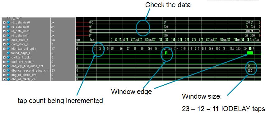
- Verify the correct Data Pattern is being read back during Read Leveling Stage 1.
The debug port includes dbg_rddata which is the captured read data.
During read leveling, a single write of the Read Leveling Stage 1 data pattern (FF00FF00FF00FF00) is sent.
This data pattern is then continuously read back.
Verify this pattern on the dbg_rddata debug signal.
If the pattern is not correct, look for stuck bits or a pattern to the incorrect data.
- Verify that the IDELAY taps are incrementing.
The idel_tap_cnt_cpt_r signal shows the tap count for the capture clock.
This value should be incremented during Read Leveling Stage 1.
- Calculate the number of edges detected.
Depending on the frequency, 0, 1, or 2 edges should be detected.
The slower the interface is running, the less edges found. A found edge is detected by the assertion of found_edge_r.
- Calculate the window size.
This is the difference in taps between the first edge detection and the second edge detection.
Look at the values on dbg_cpt_first_edge_cnt and dbg_cpt_second_edge_cnt.
The window size in IDELAY taps then equals = dbg_cpt_second_edge_cnt - dbg_cpt_first_edge_cnt.
To calculate the window size in ps, multiply the found window taps by the IDELAY tap resolution.
This is 52 ps for a REFCLK=300 MHz and 78 ps for a REFCLK=200 MHz.
- Stuck at bits (or unconnected bits on PCB)
- Unmatched traces
- Read and write leveling performed on byte basis, not per-bit
- Signal Integrity Issue that affect certain byte lanes
- Marginal signal integrity can result in a distorted capture window
- Ensure SI Simulations using IBIS are performed
- Low frequency results in non-optimal capture settings.
Continue to Read Leveling Stage 2 debug when running at low frequencies and no edges were detected.
- Wrong Pin-out
- When swapping bits some bits do not belong to the correct byte
- Moving bytes to another column without adjusting certain parameters in the RTL.
- Problems with the initial write of calibration data.
- For information on isolating a read versus a write error, see (Xilinx Answer 35209).
- Pin-Out/Banking Requirements (Xilinx Answer 34308)
- Board Layout Requirements (Xilinx Answer 34544)
链接问答记录
相关答复记录
| Answer Number | 问答标题 | 问题版本 | 已解决问题的版本 |
|---|---|---|---|
| 35209 | MIG Virtex-6 DDR2/DDR3 - Isolating a Read vs. a Write Error | N/A | N/A |
| 35206 | MIG Virtex-6 DDR2/DDR3 - Usage of Debug Port | N/A | N/A |
| 35169 | MIG Virtex-6 DDR2/DDR3 - Determining which calibration stage failed | N/A | N/A |
| 35074 | MIG Virtex-6 DDR2/DDR3 - Will calibration fail during Read Leveling Stage 1? | N/A | N/A |
| 34544 | MIG Virtex-6 DDR2/DDR3 - Board Layout | N/A | N/A |
| 34709 | MIG Virtex-6 DDR2/DDR3 - Debugging Data Errors | N/A | N/A |
| 34308 | MIG Virtex-6 DDR3/DDR2 - Verify pin-out/banking requirements are met | N/A | N/A |
