MicroZed Chronicles: Partial Reconfiguration and Block Diagrams
March 18, 2022
Editor’s Note: This content is republished from the MicroZed Chronicles, with permission from the author.
We introduced partial reconfiguration using very simple RTL a couple of weeks ago. In this blog, we are going to look at how to create a more complex partial reconfiguration example using block designs and AXI Interconnect.
This means that we want to use partial reconfiguration of a block within Vivado’s IP integrator tool. The contents of this block will be connected to the processor system using AXI4-Lite.
To get started, we are going to target the Ultra96-V2 for which a new project and a new IP integrator block diagram were created.

This was configured for the Ultra96-V2 and the following IP added SMC, an AXI Shutdown manager was configured to manage AXI commands.
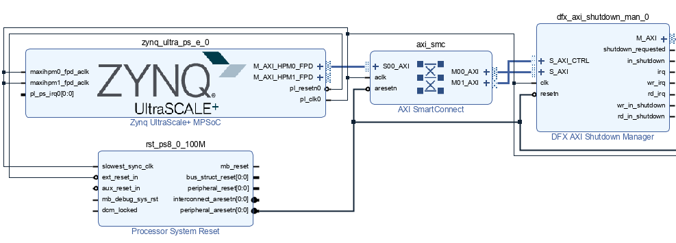
A Block RAM controller and BRAM were also added to the diagram and connected to the SMC. We then placed these inside a new hierarchical block.

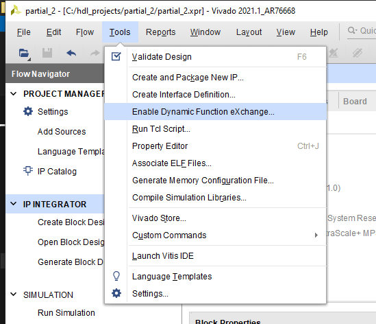
We are going to update the contents of these blocks. To do this, we first enable dynamic functional exchange on the Tools menu.
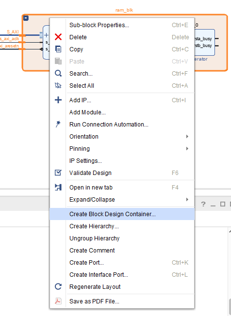
The next step is to convert the hierarchial block with the BRAM and BRAM controller into a Block Design Container. Select the hierarchical block in IP integrator and right click. Select Create Block Design Container.
This will prompt for the block name.
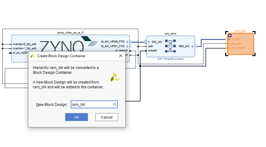
This will convert the hierarchical block into a Block Design Container. We can now set this to be enabled for DFX by selecting the sub-block properties and setting the config ENABLE_DFX to 1.
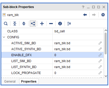
Once this is created, we can right click on the new Block Design Container and select create reconfigurable module.

At the prompt, enter the name of the new reconfigurable module.

This will create a new block diagram with the connections available.
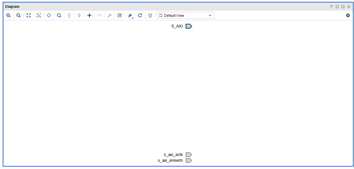
Insert another BRAM Controller and BRAM. Reconfigure the BRAM to have a COE file with a defined pattern in the lower RAM addresses.


Set the address to be the same as the address mapping as the parent. It is 0xA0000000 in this case. You should be able to double click on the Block Design Container within IP integrator back in the main block diagram. This will open the Block Design Container customization under which you will be able to see both modules assigned to it and the address ranges of the reconfigurable modules.
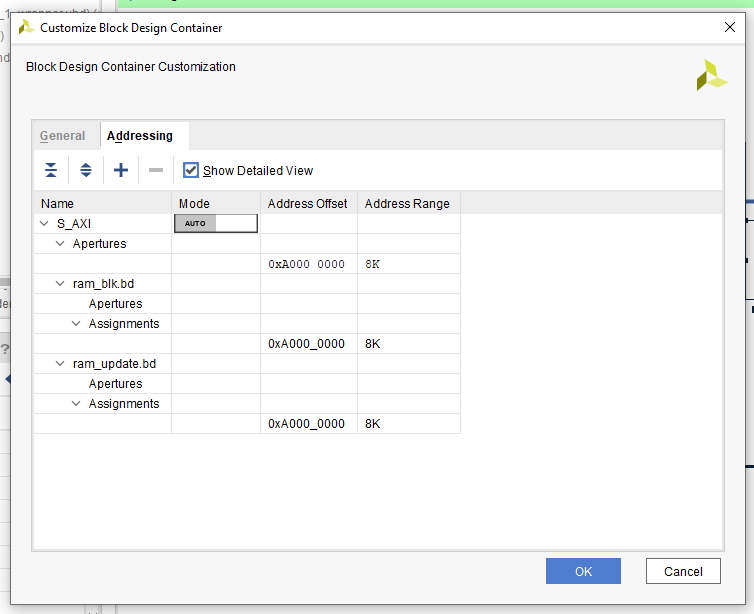
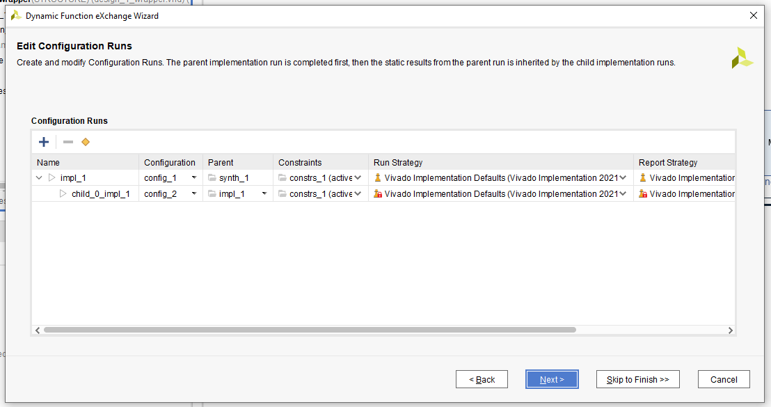
With this in place, we are then able to start running the DFX wizard as we did in the previous example. To launch the DFX wizard, make sure all the design elements are validated and generated. You should see both reconfigurable modules upon opening the DFX wizard.

The next step is to define the configurations and the run. In this case, I let the DFZ wizard automatically create both.
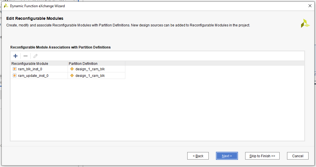
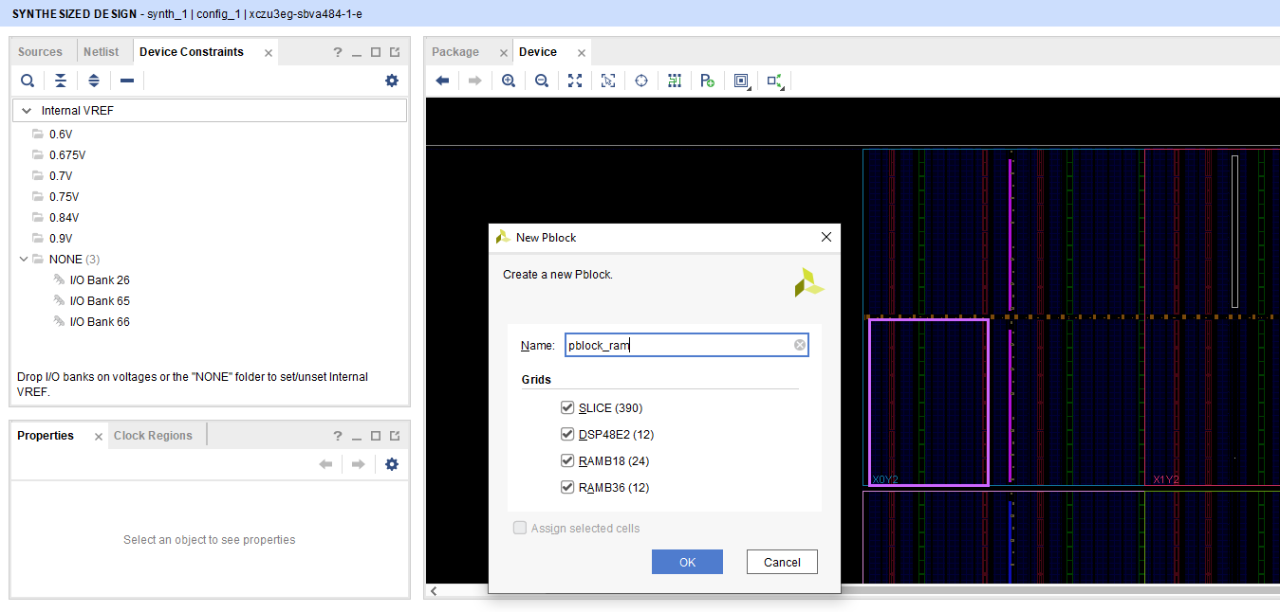
We can now synthesis the design. Once completed, open the synthesis view and create a PBlock for the reconfigurable region.
Associate the PBlock with the contents of the Block Design Container.
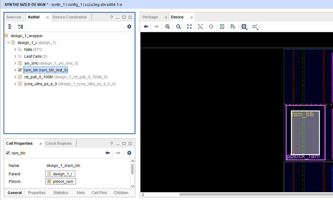
Save the new PBlock to a new XDC file to guide the implementation.

We can now complete the design implementation.
Next time we will look at how to use the AXI Shutdown to safely isolate the AXI interface so that we are able to perform partial reconfiguration of the module without the AXI interface and software crashing.
We are now well on our path to understanding partial reconfiguration.
Xilinx Xclusive Blog
-
- AMD Telecom Leadership Showcased at OFC 2022
- Mar 08, 2022
-
- 准备呐喊助威吧:赛灵思将参加 BattleBots电视系列角逐赛
- Dec 07, 2021
Adaptable Advantage 博客
Xilinx AI 和软件博客
-
- Vitis AI 2.0 现已推出!
- Jan 20, 2022
-
- 连获“双奖”,Xilinx AI 团队实力绽放国际视觉顶会
- Oct 08, 2021
-
- 您是否了解过赛灵思应用商店?评估和购买 Alveo 及 Kria SOM 解决方案的一站式商店。
- Sep 23, 2021